
A group of scientists led by Dr. Jeong-Dae Kwon and Dr. Yong-hun Kim has developed the first neuromorphic semiconductor in the world. The device has a high density and impressive reliability thanks to its thin film of lithium-ion battery. The production of ultra-thin lithium ions, popular lithium-ion batteries, and a combination of two-dimensional nano-materials helped the researchers achieve the feat. The researchers are from the Korea Institute of Materials Science (KIMS).
A neuromorphic semiconductor has neurons and synapses that mimic the human brain by processing and memorising information. The synaptic device gets signals from neurons. It also changes the synaptic weight in different ways for the simultaneous processing and storage of information. Specifically, the symmetry and linearity of synaptic weights make it possible to recognize different patterns with little power.
The making of the neuromorphic semiconductor device
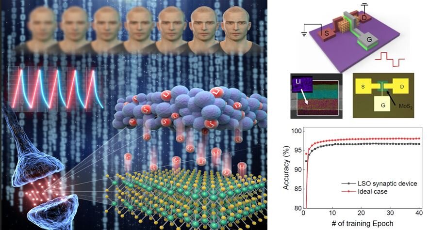
Traditional ways to control synaptic weights utilize charge traps between the interfaces of different materials. Unfortunately, it is hard to move the ions in the direction you want them to go based on the external electric field. These scientists bypassed this by making a high-density AI semiconductor device. They did this by coming up with a thin film process that kept lithium ions mobile in response to the electric field outside the device. The thin film, which is only a few tens of nanometers thick, makes it possible to make fine patterns and control how thick the wafer scale gets.
The research team made the film by using a method called vacuum sputtering deposition. This method is common in processing semiconductors. The deposited film’s thickness is less than 100 nanometers. After a silicon wafer substrate holds a transistor-like device, an electric field from the outside prompts the lithium ions to move in the charged thin film. The movement of these ions allows for control over conductivity.
Using this synapse device, the research team set up an artificial neural network learning pattern. Ultimately, it worked on recognizing handwriting image patterns. The AI semiconductor has approximately 97% handwriting pattern recognition rate by keeping the qualities of evenly adjusted synaptic weight.
Semiconductor device independent of memory and CPU
According to the research team, the semiconductor device is not dependent on CPU and memory. While it can process and store information simultaneously, it learns and identifies images such as handwriting patterns.
“Our next-generation neuromorphic semiconductor device does not require CPU and memory, the traditional Von Neumann-type information processing device and information storage device.
“ It can simultaneously process and store information and learns and recognizes images such as handwriting patterns. It is expected to be applied to various low-power artificial intelligence devices such as world-class neuromorphic hardware systems, haptic devices, and vision sensors.”
Group of researchers at KIMS about their semiconductor device
The research results were published on ACS Applied Materials & Interfaces on November 17, 2022. The collaborative research team is continuing to advance the technology of low-power AI devices and wearable edging gadgets
The featured image was taken from Techxplore
You May Also Like

Metaverse projects secure hi ...
July 4, 2023
Meta launches, Meta Quest+ ...
July 1, 2023

Baidu claims its latest chat ...
June 29, 2023